
A Flip Flop is a memory element that is capable of storing one bit of information. 2 Encoder The 4 to 2 Encoder consists of four inputs Y3 Y2 Y1 Y0 and two outputs A1 A0.

Pin On Vhdl Tutorials
The inter connection of 4 full adder in 4bit parallel adder is shown below Let us examine the justification of the above circuit by taking an example of addition of two 4 bit binary numbers.

. Half Adder and Full AdderIn half adder we can add 2-bit binary. Let us add 1011 with 1101. Design of Full Adder using Half Adder circuit is also shown.
Know all about the OR Gate here. Create circuit from truth table. Database Management System.
In particular truth tables can be used to show whether a. Mainly there are two types of Adder. They are Y 0 Y 1 Y 2 and Y 3.
From the above truth table For the different functions in the truth table the minterms can be written as 1247 and similarly for the borrow the minterms can be written as 1237. In half adder we can add 2-bit binary numbers but we cant add carry bit in half adder along with the two binary numbers. A Flip Flop is a memory element that is capable of storing one bit of information.
Based on the truth table we can write the minterms for the outputs of difference borrow. Full Adder Truth Table with Carry. The input data bit is sent to the data bit of the output lines depending on the select input or control bits value.
Advantages of Carry Look Ahead Adders. Initially first Half Adders circuit will be used to add inputs A and B to produce a partial sum. The main difference between a half adder and a full adder is that the full-adder has three inputs and two outputs.
We can also add multiple bits binary numbers by cascading the full adder. Input 1 input bit is present. The truth table of the Full Adder Circuit is shown below.
In previous tutorial of half adder circuit construction we had seen how computer uses single bit binary numbers 0 and 1 for addition and create SUM and Carry outToday we will learn about the construction of Full-Adder Circuit. The log ical exp ression for half-subtractor is. Truth Table.
A parallel adder is an arithmetic combinational logic circuit that is used to add more than one bit of data simultaneously. Full Adder is the circuit that consists of two EX-OR gates two AND gates and one OR gate. But in Full Adder Circuit we can add carry in bit along with the two binary numbers.
Single-bit Full Adder circuit and Multi-bit addition using Full Adder is also shown. Outputs The number of outputs is four. 4 a Truth Table of Full Adders Circuit b K-Map Simplification of Truth Table.
The decoder includes three inputs in 3-8 decoders. From the above half subtractor truth table we can recognize that the Difference D output is the resultant of the Exclusive-OR gate and the Borrow is the resultant of the NOT-AND combinationThen the Boolean expression for a half subtractor is as below. A truth table is a mathematical table used in logicspecifically in connection with Boolean algebra boolean functions and propositional calculuswhich sets out the functional values of logical expressions on each of their functional arguments that is for each combination of values taken by their logical variables.
For adding two 4 bit binary numbers we have to connect 4 full adders to make 4 bit parallel adder. The output carry is designated as C OUT and the normal output is designated as S. Here it is Data D.
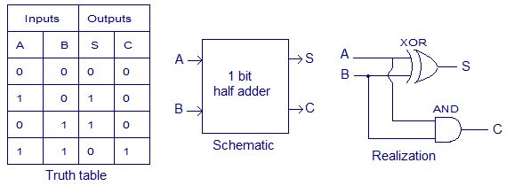
Full Adder Logic Diagram. Control Bits Two control bits are used here. If A and B are the input bits then sum bit S is the X-OR of A and B and the carry bit C will be the AND of A and B.
The first two inputs are A and B and the third input is an input carry as C-IN. A parallel adder adds corresponding bits simultaneously using full adders. The two inputs are A and B and the third input is a carry input C IN.
The Truth table of 4 to 2 encoder is as follows. A B are the input variables for two-bit binary numbers Cin is the carry input and Cout is the output variables for Sum and Carry. As the full adder circuit above is basically two half adders connected together the truth table for the full adder includes an additional column to take into account the Carry-in C IN input as well as the summed output S and the Carry-out C OUT bit.
SR Flip Flop Construction Logic Circuit Diagram Logic Symbol Truth Table Characteristic Equation Excitation Table are discussed. Karnaugh Map to Circuit. Database Management System.
Half Adder and Full Adder. This circuit can be constructed by combining two Half Adders. The logical expression for the two outputs sum and carry are given below.
Half adder is the simplest of all adder circuit but it has a major disadvantage. From this it is clear that a half adder circuit can be easily constructed using one X-OR gate and one AND gate. Half Adder and Full Adder circuits is explained with their truth tables in this article.
A 1 to 4 demultiplexer has. A full adder adds two 1-bits and a carry to give an output. The half adder can add only two.
The figure below shows the logic symbol of 4 to 2 encoder. CLA Adders generate the carry-in for each full adder simultaneously by using simplified equations involving Pi Gi. A 16 bit CLA adder can be constructed by cascading four 4 bit adders with two extra gate delays while a 32 bit CLA adder is formed when two 16 bit adders are cascaded to form one system.
They are A and B. Karnaugh Map to Circuit. The full adder is a combinational circuit so that it can be modeled in Verilog language.
However to add more than one bit of data in length a parallel adder is used. JK Flip Flop Construction Logic Circuit Diagram Logic Symbol Truth Table Characteristic Equation Excitation Table are discussed. At any time only one of these 4 inputs can be 1 in order to get the respective binary code at the output.
Mainly there are two types of Adder. A half adder adds two binary numbers. Here is a brief idea about Binary adders.
Before going into this subject it is very important to know about Boolean Logic and Logic Gates. Full Adder is the adder that adds three inputs and produces two outputs which consist of two EX-OR gates two AND gates and one OR gate. Create circuit from truth table.
As there is no previous. The Full Adders circuit can be implemented using the Truth Table and K-Map simplification.

4 Bit Ripple Carry Adder Vhdl Code Coding Ripple Carry On

Binary Adder Subtractor Construction Types Applications Electronic Engineering Electronic Schematics Engineering Technology

Binary Multiplier Types Binary Multiplication Calculator Electronic Circuit Projects Electronic Schematics Circuit Projects

Binary To Gray Code Converter 4 Bit Coding Binary Converter

4 16 Decoder Using Two 3 8 Decoders Logic Circuit Electronics Circuit

Vhdl Code For Comparator Coding 8 Bit Hobby Electronics

Vhdl Code For Full Adder

Half Adder And Full Adder Circuits Using Nand Gates Circuit Circuit Diagram Microsoft

Carry Select Adder Vhdl Code Coding The Selection Carry On

Binary Multiplier Types Binary Multiplication Calculator Binary Electronic Schematics Multiplication
One Way We Could Expand The Capabilities Of Either Of These Two Counter Circuits Is To Regard The Q Outputs As Another Set Of Four B Counter Expand Binary

Verilog Code For Comparator 2 Bit Comparator In Verilog Hdl Truth Table K Map And Minimized Equations Are Presented Coding Tutorial Writing
Difference Between Half Adder And Full Adder Coding Informative Truth

Pin On Electronic Circuit Design

Vhdl Code For Full Adder Coding Computer Science Binary Number

3 Bit Multiplier Circuit Digital Electronics Circuit

Full Adder Schenatic Electronics Electrical Electronics Circuit Electricity Electrical Components

Design 4 Bit Voting Combinational Eircuit That Has Two Outputs One Output To Indicate Mejority And Snother To Indicate A Tie Vot Homework Help Equations Logic

Kunci Jawaban Tes Koran Koran Kunci


